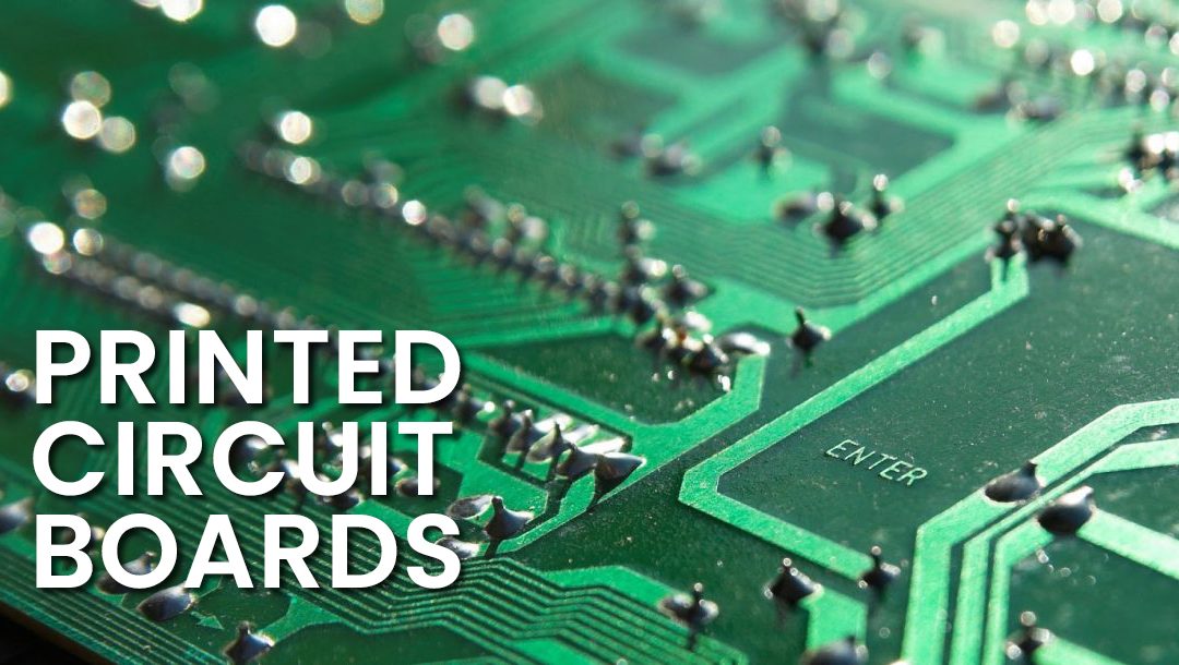
Many industries and devices today are powered by printed circuit boards in our society. With the technological advancement, the demand for different types of PCBs has also increased. The complexity of PCB fabrication has grown to align with the complexity of modern technology giving birth to single-layer, double-sided and multilayer PCB in its wake. Though be it a single layer, multilayer or double-sided PCB, it is an important subsystem to our everyday electronics. Undoubtedly the functionalities of all PCBs are different in many ways. Devices with limited functions can work well with single layer PCB while there is unlimited potential with multilayer PCBs for their collaboration with everyday new emerging electronics. From flexible to odd-shaped PCB fabrication, the range exploration is overwhelming. To ease this astounding knowledge of PCBs, let us get an understanding of the basics.
What is PCB?
PCB or Printed Circuit Board is an electric circuit board to provide mechanical support used in devices and is a pathway to its electronic components. It is created by combining different materials that are non-conductive in nature that easily supports copper-like fibreglass or plastic.
The use of multilayer PCB has grown exponentially in the current trend of technology. It came into existence to cope with changes in the electronic industry that have gone under in the last decade. Before multilayer PCB, single-layer or double-sided PCBs were the only ones to be used in the market. But due to its restricted functionality and lack of noise, stray capacitance and crosstalk limiting the performance of other devices. To overcome these hurdles multilayer PCBs were invented.
What is multilayer PCB then?
A multilayer PCB is made using three or more conductive copper foil layers. These appear to be layers of double-sided circuit boards, laminated and finally glued together with several layers of heat-protective insulation in between them. The entire construction of multilayer PCB is arranged in a fashion so that two layers are exactly placed on the surface sides of the PCB to connect to the rest of the electronic environment. The electrical connection between the layers is made through vias like plating through-holes, blinds and buried vias. Through this method and its application, a highly complex PCBs of varying sizes are created.
Multilayer PCBs are becoming more and more popular in electronics, packaging the power of a double-layer PCB into a structure that’s a fraction of the size to fit the new devices. There is a wide range of sizes and thicknesses to accommodate the right needs of their expanding applications, with variants ranging from four to twelve layers as required. Layers often come in even numbers, odd numbers of layers can cause problems in the circuit like warping. These issues can make the production unnecessarily costly. Most of the applications require somewhere between four and eight layers. Though this is not certain as mobile devices like Smartphones and Tablets tend to use around twelve layers, and some professional PCB manufacturers boast the ability of the product with nearly 100 layers. Multilayer PCBs with that many layers are pricy and are extremely rare in usage. Although multilayer PCBs are labour intensive, are specially designed by a set of specific PCB designers and are more expensive, they are the need for modern age technology. This is mainly due to the range of benefits they offer with their easy adaptability to the latest technology in comparison to single-layer and double-sided PCB varieties.
Multilayer PCB Benefits:
Multilayer PCBs are the core of the assembly of modern devices. From a technical point of view, they possess several design advantages.
Small Size: The most prominent benefit of using multilayer PCBs is in their size. The layered design of multilayer PCBs is inherently smaller than other PCBs with identical functionality. This serves as a major benefit to modern electronics, as the current trend is headed towards smaller, more compact yet more power-packed gadgets like smartphones, laptops, tablets, and wearables.
Lightweight Construction: Smaller the size lesser the weight in PCB. In the case of single-layered and double-layered PCB, multiple connectors are required to interlink separate single and double-layered PCBs. This is eliminated in multilayered design making it more compact. Being compact in nature it becomes beneficial for modern electronics that is geared more toward mobility.
High-Quality: Due to the investment of more work and planning that has to go into the creation of multilayer PCBs, multilayer PCBs tend to be better in quality than single and double-layer PCBs. Due to the investment of more time and energy in the making of multilayer PCBs, these tend to be more reliable.
Increased Durability: Multilayer PCBs also come with high durability as they are capable to withstand the heat and pressure that is applied to them. Multilayer PCBs use multiple layers of insulation between circuit layers, binding it all together with a bonding agent and protective materials which just increases there durability.
Single Connection Point: Multilayered PCBs are beneficial for gadgets where size and weight are constraints. As they possess a single connection point they become compact.
Powerful: Multilayer PCBs mostly are high density and have a greater capacity as well as speed in comparison to other variants of PCBs.
Multilayer PCBs are highly useful due to these benefits in most of the devices especially mobile phones and high functioning electronics. With the new norm of high functionality and smaller size, multilayered PCBs are highly preferred in the market.
It does possess its own set of benefits and drawbacks, though weighing the scale of pros and cons the weight is more towards the pros of these units. Yes, Today Multilayer PCBs are widely and rigorously used in most of the modern devices but they aren’t applicable to all device assembly. This limitation of multilayer PCBs is covered by single or double-sided varieties. They are expensive and need more design time, not to mention these units require skilled designers with wide experience for assembly to remove crosstalk and impedance related issues. Time investment in production is higher giving a lower turnover rate. These few drawbacks have a negligible effect in the current market that is swimming with more and more demand for multilayer PCBs. Due to an increase in the demand and supply of mobile deceives multilayer PCBs are at the peak of demand in the current market and it is certain with time its value is going upscale. Multilayer PCBs are the present and the future of the electronics market.
Hmm it looks like your blog ate my first comment (it was extremely long) so I guess I’ll just
sum it up what I wrote and say, I’m thoroughly enjoying
your blog. I as well am an aspiring blog blogger but I’m still new to the whole thing.
Do you have any tips and hints for newbie blog writers?
I’d genuinely appreciate it.
Sure. I would love to help. You can check out my website https://www.writerchi.com/