Light emission of low temperature also known as luminescence, has always existed. Luminescence comes in all kinds of forms, fireflies, or the red tide where the beach sand lights up from enchanting bacterial life form. Imagine having this luminescence to be in a controllable environment for our use. The discovery of such technology, “EL” phosphor was built on the foundation in 1936 by George Destriau who believed that zinc sulphide compound emitted light in an electric field. Years of research in the ’40s and 50’s carried out on various phosphors that would illuminate radar screens lead to modern-day televisions including LCD Displays.
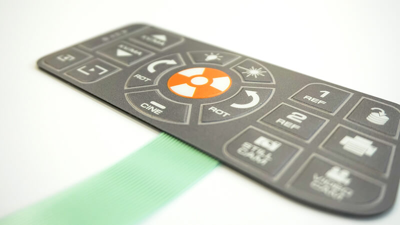
The world of EL Technology is growing at a fast pace, as the utilization is increasing with advancing technology and new products. Today EL manufacturing is done in China, Taiwan, and Singapore on large basis. It is getting more commonly used in the products sold as a current trend, products such as EL Night Lights, animated signs, EL Panels used as backlight in membrane switch keypads etc.
What is an Electroluminescent Lamp?
According to Wikipedia “Electroluminescence is an optical and electrical phenomenon in which a material emits light in response to an electric current passed through it, or to a strong electric field.” Electroluminescence serves as the building block for EL Lamps.
An EL Lamp is a LEC (Light Emitting Capacitor). These LEC lamp’s use phosphor as a key element which emits light when it is energized with an alternating electric field thus serving it’ purpose.
Electroluminescent Lamps are flat, thin along with cold illumination sources that can be refined into complex shapes. This allows them to be able to be placed into various products where space and/or power are limited. These are commonly used with backlighting products. Few examples are LCDs, aircraft instrument panels, capacitive membrane switch, and advertising signage.
Construction and Scope of EL Panels:
Electroluminescent lamps are constructed with high precision printed multiple layers of dielectric and insulated layer structure. Finishing touches are done with part-level removal and followed by connector attachments. This light technology consists of a flat capacitor construction with zinc sulphide phosphor particles between two electrodes, one of which is transparent for light to escape. When AC current is applied to the electrodes generating an electric field within the phosphor layer, causing change in the field and emitting the visible light.
As this technology is a paper-thin laminated panel they are easy to cut and have any shape. It consumes very little power and produces little heat making them ideal for use. Moreover, it doesn’t contain mechanical parts or filaments, making it unsusceptible to vibration, shock, or catastrophic failure of light. These characteristics have increased the use of EL lamps into other products, being efficient and more productive than other alternatives. Other more noticeable characteristics of EL lamps are:
- Paper Thin – Mostly between 0.25mm – 0.5mm.
- Lightweight.
- Flexibility – Can be applied to curved or flat surfaces.
- Strength – Strong as it is almost unbreakable.
- Reliability – It does not catastrophically fail as it has millions of microscopic crystals.
- Low power consumption – Consumes only between 75-90% less electricity than other light sources.
- Efficient – As 80% of the energy is easily converted to light.
- Brightness – Brightness is flexible and can be adjusted to suit customer’s requirements.
- High Visibility – It can be seen from far distances whether in darkness, smoke, and fog.
- Low operating temperature – It is a cold lighting source. It does not create heat due to its electronic luminous emission.
- No Glare – Produces a soft and even light over the entire surface area.
- It is waterproof.
- Environmentally friendly – It does not use hazardous materials.
- Longevity- Approx. 30,000 hours depending upon the usage of brightness.
- Easy to maintain, free of any surplus charge.
Benefits of EL lamps in membrane switches:
Membrane switches are found in microwave ovens, air conditioners, TV remotes, Human Machine Interfaces (HIMS), and more, almost in all the appliances we use today. Membrane keypads use cannot be fulfilled without backlighting. The backlight working is satisfied by illuminating the keys, allowing the operator of the keypad to view it clearly in darkness or in scenarios it is required. Backlighting needs a source of light, with today’s competitive market there are many. Commonly used are fiber optics or LED lights and EL Lamps. EL lamps are most beneficial while using as backlighting function for membrane keypads for its obvious characteristics mentioned above and more.
More being EL panels are cost-effective in comparison to LED or fiber optics. Other than being budget-friendly EL lamps are long-lasting. These can burn up to 16,000 hours or more, which suffices its typical usage. Agreed LED lamps can give up to 100,000 hours, more than EL lamps but being a more cost-effective solution and with another array of benefits it is a more obvious choice for most of our clients at Ranvishwa. Our other products. A noticeable advantage of this particular light tech is that even after reaching upon their half-life, these panels still work. Faded or dimmer light it maybe but they still work and it also acts as an indicator for the replacement or repairing time being near. This indication has been proven to come in handy for many of our users.
Application:
Also known as backlighting and printed light technology, EL lamps are produced in high volumes for medical, automotive, and consumer applications. The basic structure of these lights is a multi-layer printed system that is AC driven. Typical applications include
- Nightlights
- EXIT Signs
- Address signs
- Animated Point of Purchase displays
- LCD Backlights
- Keypad backlights
- Automotive instrument panels
- Digital and Analog Clocks
- Remote Control Keypads
- Automotive gear indicators.
Rangavishwa customizes Electroluminescent Lamps for all kinds of uses and applications. EL is an excellent choice for the backlighting of membrane switches. Also for the passive matrix of a monochrome display with geometrical flexibility and brightness around 30ft-l. We can design EL panels for any size, shape, or form as per your imagination.
What are Printed Electronics?
Printed Electronics are used in various applications with the advancing technology. Flexible screens, interactive books and posters, intelligent labels and packaging are made with Printed Electronics.
Printed Electronics can be stated as a set of printing methods used to produce numerous electronic devices on various substrates. Typically, electronic industries use printing equipment suitable for exemplifying patterns on different materials, like screen printing, flexography, offset lithography and inkjet. Electrically optical links are deposited on the substrates, making passive or active devices. This technology matured and unfolded its true potential over years, now inkjet printer is making inexpensive and quick printed electronic circuits.
Printed Electronics and its development
With the advancement of technology, Printed Electronics is gaining momentum. An increasing number of manufacturing industries are using Printed Electronics. Flexible screens, interactive books and posters, intelligent labels and packaging, and upholstery are being created with the use of printed technology. To fit the growing technology production lines, Printed Electronics has evolved to be thinner, lighter and more flexible. From sensors for autonomous driving or light-emitting diodes in the world of smart clothing, many such sectors depend on the lightweight and flexible electronic components. Wolfgang Mildner, CEO of the consulting and technology company MSW said, “Printed electronics has evolved into a cross-sectional and key technology.” The main focus of limelight falls on human-machine interactions and 3D-structured electronics and innovative material of this industry.
Printed Electronics has a foothold in the medical industry for many years which still is flourishing and further advancing. Sensors that help monitor various functions of bodies and micro-fluids (lab-on-a-chip) for quick test placed at the bedside used in medical diagnostics contribute to this industry. A consulting firm Mordor Intelligence assumes that printed electronics market will be widespread by almost 2023.
Aerospace yet another promising industry for Printed Electronics is still being explored. Dannis Hahn from Airbus describes the website ‘Inside Composites’ that he has carried interest in Printed Electronics for more than 20 years now. However, at that time the materials didn’t meet the safety standards for aviation used in this technology. But he saw potential which does show extreme value today, ‘a lot has changed since then’ said Dennis. Contributing to many other industries like automobiles, household machinery and more the market for this revolutionary technology is ever-growing.
Rangvishwa’s development in Printed Electronics
One of the leading manufacturers of Printed Electronics, Rangvishwa Enterprises offer several flexible printed electronics to its wide range of customer base. Providing superior quality and an array for many industries Rangvishwa has successfully launched a new member to the product line, ‘Flexible Printed Heater’. In simple words ‘Flexible Printed heaters’ are warming elements. They act as a warmth provider to appliances, clothing, products, etc. A flexible heater is a chemically etched or screen printed heater which can be flexed or bent to conform to the contours of the surface which requires heating. Polyimide/Kapton Film heaters, carbon printed heaters, and transparent heaters are some of the types. These contain the same properties on the general line as that of flexible printed electronics. Vividly growing in the garment industry due to the elasticity and flexibility of the material. Used in retail clothing and sports garments such as athlete gear, also to medical bandages, medical heating pads and more. The flexibility in the construction of Flexible Printed heaters with the advanced materials today can conform to the human body curves while giving the room for mobility, not restricting the movements in any way. As these are light-weighted, it has negligible weight to add to the garments. These properties and functionality make it ideal for its application in the garment and medical industries.
Other lines of products Rangvishwa renders are:
- Flexible Circuits
Flexible Circuits are light-weight, thin electrical circuits that can easily contour to small spaces and curvy contoured shapes. Consisting of conductive material of metal encompassed with insulating dielectric material made usually of polyimide.
- Biosensors
It is an analytical device which helps convert a biological response into an electrical signal. It is made up of transducer and biological element. Mainly used in combination of two fields’ viz. microelectronics and biotechnology.
- Printed Antennas
Also generally termed as planar antennas, these are realized with printed electronics technology. Being a part of electronic miniaturization, this product is spreading like wildfire in the technological industry. Many variants come in different geometric sizes for use in microwaves, radar transponders etc.
- In-mould Electronics
These electronics eliminate the added weight and post-processing activities by authorizing the parts to be directly included in the electronic circuitry in the process of the moulding cycle. This decorating technology works with printed electronics. Benefitting in the enhancement of manufacturing productivity, overall system cost lessens and optimizes design flexibility.
- Electroluminescent Technology
An electroluminescent film is a tool where a layer of the light-emitting phosphor is generally printed between two hugely thin electrodes, one is opaque and the other is transparent. Application of alternating current, the phosphor compound rapidly charges and discharges, resulting in the emission of light that could vary among blue, green, orange or white. Numerous other colours can be attained by adding dyes and filters to the active EL area. The electroluminescent film offers an array of advantages over other lighting sources: energy efficient, low thickness, generating no heat, providing uniform lighting with absolutely no dark areas and versatility.
- Force Sensor
Sir Franklin Eventoff discovered some materials that can change their values of resistance when subjected to force in the 1970s. These materials are called as Force-Sensing Resistors. These materials are typically used to produce a sensor that can measure the Force in a quant-able unit. These respond to applied force and convert the value into a précised measurable quantity. Used in various industries like medical, automotive, music and clothing.
Challenges faced by Printed Electronics Technology
Revolutionary tech it maybe, but with the evolving nature and expanding market Printed Electronics too, are facing challenges. Printing Technology uses printing additional layers increasing the conductivity but this leads to increased material usage and thus heightening the processing time. In the inkjet printing, the current process in use is good but not that efficient which surely is improving with the help of researchers and innovators. The industry is so new that the processes involved in the product line will keep evolving through the critical nature of the trial and error testing. This field has yet to achieve its full potential, as this is just the beginning for Printed Electronics.
Printed Electronics is a futuristic tech with a growing market. This technology with its flexibility and micro nature is contributing to the transformation of all the products it is applied to, bringing a revolution in the technology ecosystem and laying down the foundation for a technological friendly world.
]]>
What is a capacitive touch screen and how it will benefit your organization?
Remember the phrase “The World at your fingertips”, well thanks to the modern innovation of touch screen technology, the world is proverbially at your fingertips now. With just a light tap of your fingers, you can now perform a barrage of functions on account of this modern cutting-edge technology. Primarily used for smartphones, touch screen technology is now used across various electrical appliances as well. There are various methods through which an appliance will sense your touch and depending on the mechanism via which your touch is sensed there are three primary kinds of touchscreen technologies – resistive touch screen, Surface acoustic wave, and capacitive touch screen. The most widely used touchscreen technology in smartphones and other electrical appliances is a capacitive touch screen.
What is a capacitive touch screen?
In our day-to-day lives, we’re constantly using our smartphones and tablets to carry out numerous functions no matter how important menial or significant they are. Modern innovation has made our lives so much easier by letting us perform an assortment of functions by just using our fingertips but have we wondered how they work? How a mere tap of your finger will let you perform different activities like playing a game, controlling some of the switches in your house, making online transactions and much more? Have you wondered how it all works? If you’re wondering that now, the answer to wonderment is “Capacitive Touchscreen technology”. Capacitive Touch screen is a type of technology applied in a touch screen that detects a “touch” using the “capacitive coupling” method. In most of the electrical gadgets, a Capacitive touch screen is a control display with built-in sensors that help detect a touch of the human finger or a device that is specially designed for the control display, for input. The panel of a capacitive touch screen primarily contains an insulator –e.g. Glass, which is coated with a transparent conductor like indium tin oxide (ITO). Since a human body is essentially a conductor of electricity, touching the screen’s surface will distort the screen’s electrostatic field, this change in charge is measured in Capacitance. There are various kinds of technologies that can be used to ascertain the location of the touch. After determining the location, it is then sent to a controller for processing. The controller in most appliances is primarily CMOS (Complementary Metal-Oxide Semiconductor) Application-Specific Integrated Circuit (ASIC). After the controller, the information is further sent as a signal to a CMOS digital signal processor (DSOP) for processing. In the majority of the designs, the capacitance is measured by the circuits present at every corner of the panel and the information is then sent for processing to the controllers. With modern innovations, Multi-touch screens are equipped with sensors that are categorically aligned in a grid which makes it possible for the touch screens to process a more complex input. Keeping the consumer in mind, manufacturers are developing touchscreens that are thinner and with more accurate sensors. Especially for smartphones, touch screen manufacturers are now making more efficient touch screens that use “in-cell” technology that provides various benefits to the device. A prime example of this technology is the “AMOLED” screens that have a built-in capacitor in the display itself which gets rid of an extra layer inside the display, thus reducing the thickness and the weight of the display screen, which in turn is desirable to the consumer. This technology also reduces the distance between the user’s finger and the screen, thus providing efficient and more comfortable user experience.
Advantages of Capacitive Touch Screen
There are various advantages of using Capacitive touch screens in comparison to other touch screen technologies. Some of the advantages are as follows
- Conductivity – Since this technology relies on “capacitance”, the pressure applied to register a touch is irrelevant and hence it is easier to use and lighter to operate.
- Responsiveness is enhanced – The objects with which a “touch” is registered are limited and that is why there is a chance of fewer accidental interactions.
- Durability – As compared to the other technologies, Capacitive touch screens are known to be more durable and hence can be used in relatively harsh environments.
- Improved image quality – Since the display screens have glass top layers as opposed to plastic layers, the image quality in these touchscreens is much better.
- Reliable – One of the most significant advantages of this technology is that it will continue to function even with minor cracks on the screen. Display screens suffering minor cracks are one of the most common problems faced by the consumers. In the case of capacitive touch screens, the “capacitance” will still be measured even with some minor cracks in the screen, thus ensuring the smooth functioning of your device.
Disadvantages of capacitive touch screen technology.
Even though this modern innovation is highly advantageous and efficient, it has a few disadvantages. Some of which are as follows
- Unlike the resistive touch screen, a capacitive touch screen depends on conductivity and hence in some cases, a touch screen may not detect the touch of a glove since some gloves are insulators and do not conduct electricity. It also requires special stylus that are conductors of electricity
- In comparison to a resistive touch screen, a capacitive touch screen tends to be a tad expensive
- Since a capacitive touch screen contains a glass display screen, it is prone to breaking or cracking and hence requires a protective guard to protect the display screen
Uses of Capacitive touch screen
Due to its efficiency and other advantages, Capacitive touch screens are used in almost every smartphone today. It is also used in various tablets, Microsoft Surface laptop, Apple Ipads, Iphones, and Ipods.
How will the Capacitive touch screen benefit your organization.?
Smartphones along with other electrical appliances that employ touch screen technology are now an essential part of our lives. Whether you are a consumer or a business, you use a touch screen device in your day to day life. Whether you own a restaurant where you can quickly take your orders on a tablet or a smartphone, whether it is a ticketing kiosk where tickets can be bought by entering your information and paying through an Automatic Ticket Vending machine, a touch screen device with a capacitive touch screen will particularly be beneficial to you and your organization. Some of the benefits it will bring to your organization are as follows
- Capacitive touch screens are highly sensitive and maximize accuracy with potent sensors that more accurately detect your touch and hence it makes your work even more efficient and saves you a lot of time.
- It requires less pressure to use which will provide a relatively longer shelf-life to your device
- It provides a better display and higher resolution hence ensures a better consumer experience.
- Capacitive touch screen technology can also be used for Multi-touch touch screens which will help you perform various complex functions on your device
Capacitive touch screens with their dynamic functions and numerous advantages have truly ushered in a new area when it comes to touch screen technology. Employing this technology for your organization will be highly advantageous. Whether you are a consumer or a business, capacitive touch screen technology will provide you the best possible experience while dealing with touch screen devices
]]>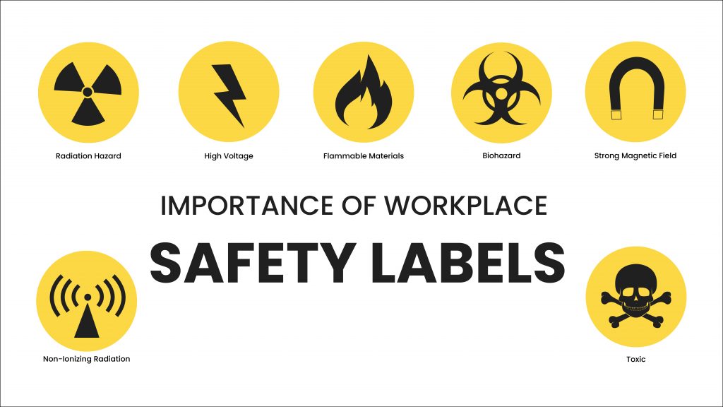
Working with heavy machinery, hazardous chemicals, and electrical equipment can be dangerous and there are potential risks involved that may lead to critical injuries. To avoid a mishap or serious injuries companies are required to practise various safety measures as described by the guidelines of various worker unions and government agencies. Undertaking proper safety protocols is essential to ensure the safety of the employees. Safety measures are critical to inform the employees and visitors of the potential risks and injuries that may be caused at the premises. The safety measures also help the employees in exercising caution when handling equipment and areas that may pose a danger. Various safety measures need to be implemented but one of the most elemental measures is “Safety Labels”.
What is a safety label?
A safety label is a label attached to an item or present in its instruction manual, which warns the users about the potential risks and dangers of using the said item. There are various types of safety labels depending on the aspect of the company. In an industry that operates heavy machinery, hazardous chemicals or electrical equipment, it is important to label each machine with the proper information to avoid potential accidents.
Importance of safety labels in the workplace.
- While working with certain machinery, chemicals, electrical equipment there are major chances of accidents that may cause fatal injuries. Various labour organizations across the globe have come up with numerous laws to ensure employee safety. A critical part of the labour laws across the globe is putting “Safety Labels” across areas of the company where there is a risk of potential injury. Numerous studies have concluded that having a visually attentive sign is key to ensure employee safety in the workplace. An organization like OSHA (Occupational Safety and Health Administration) in the United States has provided certain protocols for putting safety labels to ensure workplace safety that is mandatory. An organization like the American National Standards Institute (ANSI) has provided various guidelines on how the safety labels should be implemented. ANSI explicitly states that a safety label should contain an image on the label, called as a pictogram, which is a visual representation of the potential hazard of using the said machine. ANSI further states that the label must also have a signal word that alerts a person regarding potential hazards. Some of the signal words, along with its corresponding colours, to alert the reader as per ANSI Z535 safety standards guidelines are giving below:
- DANGER: The word “Danger” should be written in white and surrounded by red. It is to be used in situations that will result in critical injuries or possible death. The “Danger” signs are to be used in the most serious conditions.
- WARNING: The word “Warning” should be written in black and surrounded by orange. It is to be used in situations with potentially serious hazards or death.
- CAUTION: The word “Caution” should be written in black and surrounded by yellow. It is to be used in situations where there is a potential injury that can be described as minor to moderate. They can also be used effectively as an alternative to NOTICE signs.
- NOTICE: The word “Notice” should be written in white and surrounded by blue. It is used to alert the viewer regarding safety rules and procedures regarding a certain area or safety procedures while operating certain equipment. It is also used to convey other information in situations where there is no potential hazard.
Along with the aforementioned safety words on labels, there may also be short sentences that convey the message of safety quite efficiently. The message may also be effective in conveying the nature and possible consequences of the hazard and measures that serve as a precaution against the potential hazards.
Implementing safety labels not only saves time but boosts productivity by relaying the necessary information regarding the caution that needs to be exercised. An alert employee will also be more productive in his/her area once he/she is aware of all the safety protocols.
Types of Safety Labels
Depending on the nature and aspect of the industry, various safety labels can be implemented within the workplace. Some of the types of safety labels are given below:
- Machine Safety Labels: Operating with heavy machinery and/or electronic equipment poses a potential risk of numerous injuries. Having a clear visible Label on the machine that describes the proper protocol of the machine’s operation, its potential risks, and information on how to avoid the potential hazards, can be very effective to safeguard the employee’s safety. Over a period of time, the labels tend to get worn out or torn off rendering the employee incapable of reading the signs. It is important to consistently renew these safety labels with labels made from durable material like polycarbonate, polyester, foil or vinyl.
- Building or facility safety labels: These are some of the most common safety labels found in the workplace. These labels are usually posted in areas of the company where the employee should exercise certain precautionary measures like watching their step in certain areas, keeping doors closed in certain departments, being alert regarding low-hanging equipment, always wearing the proper footwear, clothing, and protective gears. The protocol for these kinds of safety labels is a bit flexible when it comes to ANSI guidelines and specifications. However, it is recommended that the safety labels contain the necessary information like a pictogram, signal words, etc. in order to relay the fundamental safety instructions.
- Emergency exits and Fire equipment: Safety labels related to fire safety and regulations are absolutely vital to the workplace. There are certain protocols and codes when it comes to the safety labels that relay information regarding fire safety and these Safety Labels are monitored by the local fire department on a regular basis. The protocol states that the Texts on the label should always be in capital letters and in red colour. The pictogram must indicate the proper procedure of fire safety protocol. The EXIT signs should be illuminated from behind, clearly visible and should be located above the entryways that lead outside and which can be used in case of a fire or other related calamity.
Safety Labels are absolutely essential to safeguard employees from potential risks of injuries at workplaces. There are various guidelines and protocols laid out by Labour organizations that help safeguard the employee’s safety. Safety Labels around the workplace are an efficient practice that will help prevent critical injuries. An employee who feels safe at the work environment will be more productive in his field
]]>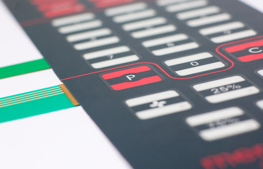
Membrane switch technology made it possible for companies to develop more convenient gadgets. Washing Machines, Microwaves, Television and various other devices work on the same technology. Compared to mechanical switches Membrane switches offer a softer feel. As the switch is more sensitive, users can easily change functions or shift switches. You can change operations and complete tasks without exerting much effort. The switch is also leak-proof and waterproof. This makes the technology ideal for businesses operating with harmful components in harsh environments.
Membrane switches are touch-sensitive devices developed by the printing, cutting and laminating of precision thin-film plastic materials. Low-voltage, low-current momentary electrical contact is made and retained by applying finger-tip force to the front surface of the switch. Membrane switches are primarily used with microprocessor-based control systems found in communication, medical, instrumentation and appliance products.
A number of industries now prefer Membrane switches technology for front panel solutions where frequent contact with water is an issue due to its sealed nature coupled with its reliability and ability to offer tremendous aesthetic flexibility. The technology although sophisticated is very simple to create at home and renders fairly effective. Let’s have a look at how to create membrane switches from the scratch
Step 1: Understanding the Keypad
The first thing to understand is how this keypad works. A matrix style keypad is a grid consisting of rows and columns and each button corresponds to a certain row and column. A 9 button keypad, will use 3 rows and 3 columns. The first button connects the link between Row 1 and Column 1 (R1C1) just like in battleship. 2 would be R1C2, 3 R1C3, and 8 would be R3C2. The main reason to do this is instead of having 9 different buttons to wire up, you would only need to wire up 3 columns and 3 rows for significantly fewer wires. This is very beneficial when you begin adding buttons. Adding one more row and column (2 wires) will add 7 buttons.
Step 2: Collecting Materials.
The best thing about this instructable is you probably already have all the things you need to build this in your house. This is a cheap, simple, and effective way of making a membrane keypad. You will need:
- Aluminum Foil *foil tape works too.
- Some sort of paper or flat material (what you choose here will affect the durability.)
- Glue (unless you’re using foil tape)
- And a spacer of some sort (a few layers of paper with holes cut in them may work I’m using double-sided sticky foam pads)
Step 3: Decision Time
Before everything else you have to decide what you want your keyboard to look like/how many buttons do you want on it. For this instructable, you can use a 3X3 setup with the numbers from 1 to 9 on it. Once you have finalized the look, draw it and decide where you want all the wires to go. Make a mock-up on your computer using any design software you like for e.g. Paint, Photoshop, and Illustrator and proceed to the next step.
Step 4: Mapping Out Your Cheap “Circuit”
We are going to be glueing on foil to make a flexible, cheap, however effective circuit board. What we need to do now is on our computer mockup we need to make how our columns and rows are going to be set-up. If you are using Photoshop make 2 new layers, one called rows the other columns. If you’re just using paint make a copy of the file called rows and another column.
We will put large black lines on these new layers, where we want our “Circuits” to go.
Now you need to flip one of your images vertically. Go ahead and print these out for the next step.
Step 5: Faux Circuit Making Time
Now that you have your printed templates you can start making your circuit. This is when you glue your foil where your rows and columns are supposed to go.
*NOTE* At this point it’s a good idea to re-make your front design to include labels for the hookup at the end of the leads with the labels. R1, R2, R3, C3, C2, C1. This is just going to make it easier for you.
Step 6: Final Assembly
In the next step, we will be putting it all together. Take your spacers and apply them to one side of your keypad. You could use silicone technically, the type used for caulking, as a really decent spacer. To apply these spacers we need to make sure that there is a hole in the centre of them so that the rows and columns can contact one another when they are depressed. You could use a hole-punch to get better results. The spacers make sure that other parts of our circuit do not come in contact with each-other incidentally.
Once your spacers have been applied, you may need to glue whatever you are using and put the other side of your keypad on top of this one. You have already made sure that everything was mapped out precisely on your template you designed on your computer.
Optional Step
To help your keypad enjoy a long healthy life, laminate it. It helps to provide structural support for the paper. Constant pressing can and will create depressions in the paper that sooner or later will cause your keypad to become ineffectively pressurize that button constantly.
]]>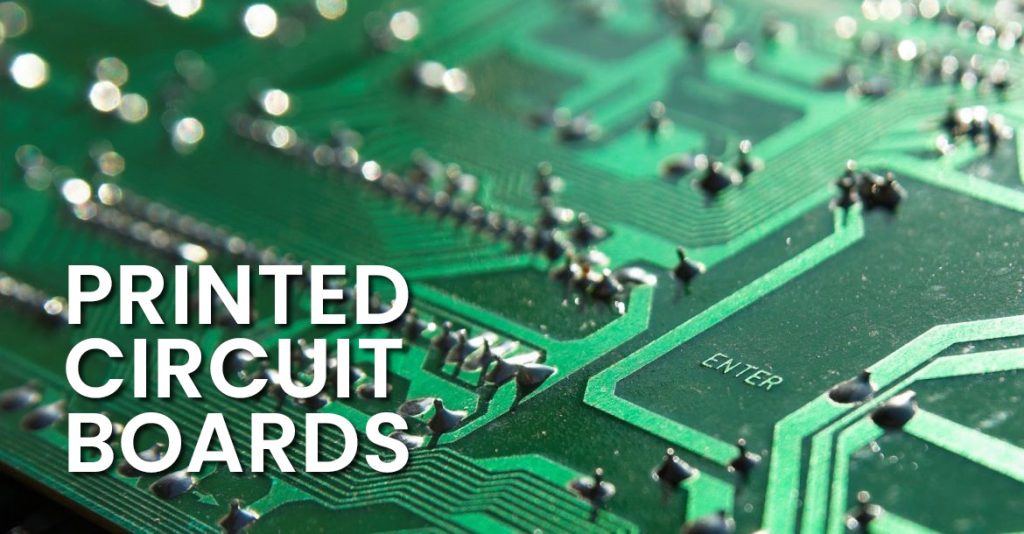
Many industries and devices today are powered by printed circuit boards in our society. With the technological advancement, the demand for different types of PCBs has also increased. The complexity of PCB fabrication has grown to align with the complexity of modern technology giving birth to single-layer, double-sided and multilayer PCB in its wake. Though be it a single layer, multilayer or double-sided PCB, it is an important subsystem to our everyday electronics. Undoubtedly the functionalities of all PCBs are different in many ways. Devices with limited functions can work well with single layer PCB while there is unlimited potential with multilayer PCBs for their collaboration with everyday new emerging electronics. From flexible to odd-shaped PCB fabrication, the range exploration is overwhelming. To ease this astounding knowledge of PCBs, let us get an understanding of the basics.
What is PCB?
PCB or Printed Circuit Board is an electric circuit board to provide mechanical support used in devices and is a pathway to its electronic components. It is created by combining different materials that are non-conductive in nature that easily supports copper-like fibreglass or plastic.
The use of multilayer PCB has grown exponentially in the current trend of technology. It came into existence to cope with changes in the electronic industry that have gone under in the last decade. Before multilayer PCB, single-layer or double-sided PCBs were the only ones to be used in the market. But due to its restricted functionality and lack of noise, stray capacitance and crosstalk limiting the performance of other devices. To overcome these hurdles multilayer PCBs were invented.
What is multilayer PCB then?
A multilayer PCB is made using three or more conductive copper foil layers. These appear to be layers of double-sided circuit boards, laminated and finally glued together with several layers of heat-protective insulation in between them. The entire construction of multilayer PCB is arranged in a fashion so that two layers are exactly placed on the surface sides of the PCB to connect to the rest of the electronic environment. The electrical connection between the layers is made through vias like plating through-holes, blinds and buried vias. Through this method and its application, a highly complex PCBs of varying sizes are created.
Multilayer PCBs are becoming more and more popular in electronics, packaging the power of a double-layer PCB into a structure that’s a fraction of the size to fit the new devices. There is a wide range of sizes and thicknesses to accommodate the right needs of their expanding applications, with variants ranging from four to twelve layers as required. Layers often come in even numbers, odd numbers of layers can cause problems in the circuit like warping. These issues can make the production unnecessarily costly. Most of the applications require somewhere between four and eight layers. Though this is not certain as mobile devices like Smartphones and Tablets tend to use around twelve layers, and some professional PCB manufacturers boast the ability of the product with nearly 100 layers. Multilayer PCBs with that many layers are pricy and are extremely rare in usage. Although multilayer PCBs are labour intensive, are specially designed by a set of specific PCB designers and are more expensive, they are the need for modern age technology. This is mainly due to the range of benefits they offer with their easy adaptability to the latest technology in comparison to single-layer and double-sided PCB varieties.
Multilayer PCB Benefits:
Multilayer PCBs are the core of the assembly of modern devices. From a technical point of view, they possess several design advantages.
Small Size: The most prominent benefit of using multilayer PCBs is in their size. The layered design of multilayer PCBs is inherently smaller than other PCBs with identical functionality. This serves as a major benefit to modern electronics, as the current trend is headed towards smaller, more compact yet more power-packed gadgets like smartphones, laptops, tablets, and wearables.
Lightweight Construction: Smaller the size lesser the weight in PCB. In the case of single-layered and double-layered PCB, multiple connectors are required to interlink separate single and double-layered PCBs. This is eliminated in multilayered design making it more compact. Being compact in nature it becomes beneficial for modern electronics that is geared more toward mobility.
High-Quality: Due to the investment of more work and planning that has to go into the creation of multilayer PCBs, multilayer PCBs tend to be better in quality than single and double-layer PCBs. Due to the investment of more time and energy in the making of multilayer PCBs, these tend to be more reliable.
Increased Durability: Multilayer PCBs also come with high durability as they are capable to withstand the heat and pressure that is applied to them. Multilayer PCBs use multiple layers of insulation between circuit layers, binding it all together with a bonding agent and protective materials which just increases there durability.
Single Connection Point: Multilayered PCBs are beneficial for gadgets where size and weight are constraints. As they possess a single connection point they become compact.
Powerful: Multilayer PCBs mostly are high density and have a greater capacity as well as speed in comparison to other variants of PCBs.
Multilayer PCBs are highly useful due to these benefits in most of the devices especially mobile phones and high functioning electronics. With the new norm of high functionality and smaller size, multilayered PCBs are highly preferred in the market.
It does possess its own set of benefits and drawbacks, though weighing the scale of pros and cons the weight is more towards the pros of these units. Yes, Today Multilayer PCBs are widely and rigorously used in most of the modern devices but they aren’t applicable to all device assembly. This limitation of multilayer PCBs is covered by single or double-sided varieties. They are expensive and need more design time, not to mention these units require skilled designers with wide experience for assembly to remove crosstalk and impedance related issues. Time investment in production is higher giving a lower turnover rate. These few drawbacks have a negligible effect in the current market that is swimming with more and more demand for multilayer PCBs. Due to an increase in the demand and supply of mobile deceives multilayer PCBs are at the peak of demand in the current market and it is certain with time its value is going upscale. Multilayer PCBs are the present and the future of the electronics market.
]]>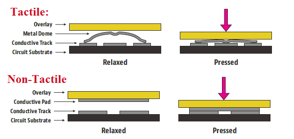
What is the Basic Difference Between Tactile and Non-tactile Membrane Switches?
After membrane switches and keypads were invented, they weren’t trusted to be the best quality method of inputting data. Though with the passing time membrane keypads and switches have had a huge transformation in their perceived image and have stood positively to the test of time. Now they are proven to be one of the best cost-effective and reliable input methods for many different applications. Due to the unquestionable benefits and advantages, these high technology subsystems have become irreplaceable to many industries. Mainly two types of membrane switches are used in the market, classified into tactile membrane switches, and non-tactile membrane switches. These switches can also be used by mixing and matching according to their functionality in the very same panel. A printed circuit board can be opted to use for the lower circuit to provide structural support in addition. These switches play an equally important role in modern technology, though they are different in many ways, the functionality, construction, and uses of these tactile and nontactile membrane switches are different in minimalistic yet significant ways.’ How exactly tactile and non-tactile membrane switches are different if the differences are minute?’ Let’s discuss that in detail.
Construction of Tactile and Non-tactile Membrane Switches:
The construction is almost the same as the tactile and the non-tactile membrane switch. In the construction of the tactile membrane switch, there is a metal dome just below the surface of the overlay. Whereas in non-tactile membrane switch there is a conductive pad instead of a metal dome, again just below the overlay layer.
With the tactile membrane switch, the user gets tangible feedback when the button has been pressed. The metal dome once pressed provides momentary contact with the circuit layer. It is supported by the adhesive spacer layer and in the relaxed state, the dome legs rest on the outer rim of the primary pathway. When pressed, the dome makes contact with the secondary pathway right in the center, thereby completing the loop of the circuit. Materials like stainless steel, polydome or hydroform can be used to make these switches, in addition, it can be activated more than a million times.
While with the non-tactile membrane switch, separate feedback to the user is used to confirm activation. The activation can be done with light, sound or visual display. Non-tactile membrane switches are comparatively more reliable and have a high durability stand. It can be activated up to five million times in its life cycle.
The Functionality of the Tactile and Non-tactile Membrane Switches:
Tactile membrane switches are usually internally vented and are sealed from the environment surrounding it. This makes it stronger against contamination from outside particles making it useful for the medical industry. The tactile membrane switches is a momentary switch. Its construction defines its functionality. The significance of the construction is when it is pressed, the action is set into a flow and when the pressure is released the action flow stops. Its use can be easily understood through the example of keyboard switches, out of many of its functionalities. In the case of keyboard switches when the letter or symbol is pressed the action is inflow and the letter or symbol appears on the screen. And when the pressure is released the letter or symbol stops appearing as the action is stopped.
Non-tactile membrane switches are used to activate objects like backlighting of the control board monitor. When the button is pressed nothing appears on the monitor screen, instead an LED light will turn on or a beeping sound will occur to indicate that the activation has been done. These are just a few examples, elaborating one of the functions of these membrane switches out of many functions.
Uses of Tactile and Non-tactile Membrane Switches:
Tactile switches are sealed and usually vented internally making them preventive to outside particles in the surrounding environment. Due to this quality, it has been widely adopted by the medical industry. These switches carry out a small number of functions, are easily integrated with portable devices and have optimal visibility, additionally, lightweightedness adds to its value for medical industry devices. Throughout the medical facilities, these devices are used like hospital bed controls, ultrasound systems, monitoring equipment, thermostats and many more. These switches are vulnerable to bacterial attacks or cleaning products, making it essential for the use of materials that can be resistant to these infectants, making them ideal for healthcare or medical facilities. Non Tactile membrane switches are whole self-accommodated units that do not provide feedback. Often supported by audio signal or visual display to ease out the use for the operator. Most commonly seen in microwaves, these switches give a beeping sound to indicate that action has been activated. It allows keypad shaping and sizing customization which makes it most preferable for designers and engineers in general. The transport industry hugely uses non-tactile membrane switches at gas stations and vehicle speedometers. Speedometers do not require any tactile input but need to constantly show the levels of speed as the user drives the vehicle. These switches are customized with embossing and backlighting function to provide more clarity to the rider. These are user-friendly and cost-effective designs.
Be it tactile or non-tactile membrane switches both have their significant roles in technology today. Widely used in many industries, they have been proven to be highly customizable subsystems for the evolving technology. Each one comes with its own set of pros and cons, it depends upon the manufacturer the usability of the switches and with that its application. Though we can state this with the assurance that both membrane switches are in technology for a long haul.
]]>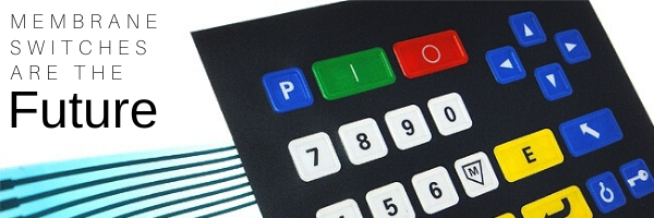
Technology has moved forward leaps and bounds in a small span. Membrane keypads and switches are innovative inventions of this technologically advanced era. Membrane keypads and switches are the functional and aesthetic user interface between the software and hardware control systems. We use these keypads in our daily lives, washing machines, dishwashers or microwaves operate through membrane keypads. The smaller and less clunky technology is, the better usage it generates. Membrane keypads and switches are examples of such advanced technology, bringing easy solutions to modern-day problems.
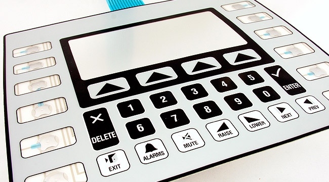
What are Membrane keypads and Switches?
Membrane keypads or switches are a whole, non-separate pressure design pads that have only outlines and symbols printed on a flexible flat surface. They function with electrical contact between the keypad surface and underneath circuits when the symbols on the keypads are pressed. The basic principle of functionality is that the contact behind the tactile key or non-tactile key closes an open loop of the circuit which terminates on the flexible tail (FPC). They are used in domestic and industrial applications on a wide variety. It ranges from backlit keypads, embossed versions, capacitive touch fascias and much more. They are customized to the customers’ individual requirements. A number of industries, electronics, white goods, medical, security and marine use membrane keypads and switches.
Benefits of Membrane keypads and Switches
Design: The design of membrane keypads and switches are created in a manner to keep them free of dirt and grime. It is a fully sealed surface, which is easier to clean and maintain. As there is no coagulation of any dirt or grime, the circuits function smoothly, making them more durable and sturdy in nature. Some of the designs are waterproofed. Adaptive designs are created to suit different customers according to their specific needs.
Versatility and Flexibility: The designs are adaptive to the specific needs of the buyer, designs are made to suit a specific product. The graphic overlay, symbols, material of the membrane keypad or switches, functionality, precise color to match the product and other specifics are for the customer to choose. An array of different industries as well as domestic sectors use membrane keypads and switches. From gym equipment like treadmills or domestic appliances like a washing machine to marine machinery, membrane keypads and switches are used on a varied scale. The material used for manufacturing isn’t rubber so they can be easily printed digitally, giving accurate and crisp graphics integrated with LED or with backlit membrane keypads and switches. Tactile or non-tactile whichever suits the clients’ needs. Flexible in size, to fit any machinery or product for use.
Durability: The material used to make these membranes vary according to budget and the functionality in regards to the product. Materials like Polycarbonate (also known to be Lexan) or Polyester (PET) are used for the production. Polyester is a bit expensive and is used where perks like heat stability for low resistance, raised keys, laser cutting is required. Polycarbonate is more an aesthetic choice, Ink keying, dye cutting, and forming are simple to create with this material. Cost-effective Polycarbonate won’t be effective while using solvent-based chemicals. Membrane keypad and switches being completely sealed offer easy cleaning and durability. Some offering waterproof material, some dust and grime free materials ensuring a longer life span. The membrane keypads and switches also have sub-surface graphics (printing is on the underside of the membrane) so that in time the visuals don’t degrade and cleaning won’t fade away the symbols. Keeping the identity of graphics alive for a longer duration. Adhesives are used to keep the material of the membrane keypad or switches in mind as well as the product they will be mounted on.
Enhanced Protection: Other than being extremely durable membrane keypads and switches have the advantage of providing better protection to the product it has been mounted on. Its design servers to be waterproof which can protect your machinery from any water or liquid mishap that might happen. Let’s consider a treadmill, people drink water or protein shakes while workout sessions and the entire machinery is only vulnerable from where it is operated. Using a waterproof material for treadmills membrane keypad can protect the owner from the huge bill for repairing with any liquid mishap. Similarly, membrane keypads and switches can survive harsh UV lights where other types of machinery are damaged by exposure. Also, they are resistant to few chemicals making these a full protection package, ideal for your machine. Guaranteed protection with different materials just to suit your needs.
Cost-effective and Easy Repairs: Membrane keyboards are inexpensive and are resistant to dirt and liquids the other keyboards making them ideal for use. These are much easier to repair in comparison to other mechanical keyboards. The circuit design with an overlay makes the process of the membrane keypads and switches much easier. In case of damages, you can easily remove the overlaying membrane, correct the damages in the circuit and simply place back the overlying membrane to make it fully functioning again. Cost-effective as well as simple to repair or modify where the product has an issue with the membrane keypads and switches. The easy repairing makes it so versatile in so many industries.
Membrane keypads and switches are Cost-effective full package deals, which is getting better and updated day by day to fit the ever-advancing technology. Membrane keypads and switches have brought significant changes in technology since its application from the early 1980s on home computers. Today it is widely used in normal computer keyboard as well with an array of dome switches just to give positive tactile feedback. As widespread the use of membrane keypads and switches is today, we can easily say it is one of the revolutionary inventions of modern times
]]>